Home > Tech Tools > Technical Papers > A Low-Inductance DC Bus Capacitor for High Power Traction Motor Drive Inverters
Virginia Polytechnic and State University
668 Whittemore Hall
Blacksburg, VA 24061-0111
Electronic Concepts, Inc.
526 Industrial Way West
Eatontown, NJ 07724
ABSTRACT
For a battery-powered traction motor drive, the inverter dc bus presents high-frequency pulsating current due to device switching. Conventional inverter design sizing dc-bus capacitor based on voltage ripple is no-longer effective. In order to handle high current in high temperature environment, a low- inductance high-current film capacitor is proposed to replace the conventional electrolytic bulk capacitors for a 75-kW traction motor drive inverter. The proposed design results in significant size reduction and performance improvement over the existing one. Characteristics of the low-inductance high- current film capacitor are presented to show its superiority to the conventional electrolytic capacitors. Experimental results are shown to verify the need of the proposed capacitor.
Key Words: capacitors, traction motor drives, inverter design
I. INTRODUCTION
Recently the capacitor technology has been getting more and more attention in industry. For low power applications, especially in computers and telecommunications, the selection criteria and availability have been discussed and summarized in [1]. For traction motor drive applications, the life expectancy of dc bus capacitor has been discussed in [2]. With a successful development of using a newly developed low-inductance high-current film capacitor in a high power (75 kW) traction motor drive, the intention of this paper is to provide the theoretical background and field experimental data for a potentially better dc bus capacitor design option.
The dc bus capacitor is the most important passive component in a traction motor drive. Conventional designs have been using a set of electrolytic bulk capacitors to smooth dc bus voltage. It was found through dc bus voltage and current ripple study that a single low-inductance high frequency film capacitor could be used to replace our original 75-kW traction motor drive inverter design that used three bulky electrolytic capacitors. Significant results are (1) size reduction, (2) cost reduction, and (3) reliability improvement. With the use of the proposed high power film capacitor, the entire traction motor and inverter can then be integrated into a compact housing, eliminating substantial amount of cables and their associated cost and losses.
The dc bus capacitor in high power traction motor drives need to deal with the following problems: (1) the ripple current due to inverter switching, (2) voltage fluctuation due to the source lead inductance, (3) voltage transient due to leakage inductance and fast device switching, and (4) over voltage due to regeneration. The capacitance needed to deal with the first three problems may not be high, but the current handling capability and frequency response of the capacitor are the major concerns. For the regeneration, if the battery is directly connected to the dc bus, then the size of the capacitance is not an issue. Thus, the overall design should focus on the current handling capability in a wide temperature environment.
Our traction motor drive inverter has been going through a few generations. In our first generation inverter design, the dc bus consists of four electrolytic capacitors with each rated 450 V, 6,800 μF. In our second-generation inverter design, the dc bus consists of three electrolytic capacitors with each one rated 450 V, 4,700 μF. The size of each second- generation inverter capacitor is 3” diameter by 5.125” tall, and the ripple current capability is 12.3 A at 85°C [3]. With three of them in parallel, the total current capability is only 36.9 A. Although the rating seems to be low, the reason for allowing the capacitance and size reduction is because the entire inverter including the capacitor was cooled by a 26-W fan, and the temperature did not exceed the limit. The dc bus voltage ripple has never been an issue throughout the design of the first two generations.
For the new generation, the inverter design idea is to integrate the inverter and motor together with one set of liquid cooling so that the size and weight of the entire traction motor drive can be further reduced, and thus the driving range can be further extended. Therefore, the newly developed traction motor drive inverter adopts one 500 V,200 μF film capacitor to replace the original bulky electrolytic capacitors. With the physical size of 3.6” × 4.5” × 1.4”, this capacitor has a ripple current capability of 140 A at 85°C. Thus this new inverter not only reduces the physical size, but also improves high-frequency ripple current handling capability.
In addition to significant improvement in ripple current capability and size reduction, the newly adopted low- inductance film capacitor also demonstrated significant voltage spike reduction over the conventional design that used the combination of power bus bar and bulky electrolytic capacitors. Our second-generation bus bar-based inverter with three electrolytic capacitors showed more than 33% voltage spike during the device turn-off transient. With the low inductance film capacitor that is integrated with a thick copper printed circuit board (PCB), the voltage spike is reduced to 14%, allowing elimination on additional dc bus snubber capacitors.
It is also well known that the electrolytic capacitor has limited life expectancy because its electrolyte tends to dry out after 10,000-hour usage. Substituting the bulky electrolytic capacitor with the film capacitor allows the life expectancy to be extended to more than 100,000 hours – an order of magnitude improvement.
In this paper, the complete circuit diagram of a traction motor drive inverter circuit will be described in detail for the cause of current ripple and voltage spike, and thus justifying the need of low inductance film capacitor. Based on the inverter voltage and current information, the specification of the dc bus capacitor can be determined, and the type of the capacitor can be selected. The characteristics of the selected film capacitor will be shown to see if it meets the design requirement. Photograph of a 75-kW traction motor drive inverter power section will be shown to indicate all the associated components and its low parasitic inductance nature. Finally, the experimental results will be shown to indicate the superiority with the use of the proposed high- current low-inductance file capacitor.
II. INVERTER CIRCUIT AND CAPACITORS NEEDED
Fig. 1 shows a simplified circuit diagram of the battery- powered inverter for a three-phase ac motor drive. According to this circuit, only one capacitor is needed. Strictly speaking, even this capacitor is redundant because it is paralleled with a stiff dc source. The question is why and what type of capacitor is needed with such an argument. To answer this question, it is necessary to have a good understanding of inverter switching mechanism and circuit parasitic components.
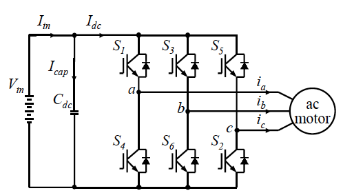
Fig. 1. Simplified inverter circuit diagram.
The synthesis of a smooth sinusoidal current for the ac motor drive with a stiff dc voltage source is to have high rate of switching in different combinations of the inverter switches so that the output current can track a desired sinusoidal current to reduce the ripple content. This ripple magnitude is a function of the dc voltage, motor inductance, motor back electromagntic force (emf), and the switching period. Every switching period has a voltage across the motor winding either +Vdc, 0, or –Vdc. When a +Vdc is applied, the motor current rises. On the other hand, when 0 or –Vdc is applied, the motor current falls. The switching frequency in today’s insulated-gate-bipolar-transistor (IGBT) based inverter is typically between 10 kHz and 20 kHz. Depending on the motor winding inductance and the modulation scheme, the ripple ranges from a few percentages to near full-load current. In an induction motor-based EV traction drive, this ripple is around 25 to 65% of the rated load current. In a permanent magnet motor-based EV traction drive, the ripple is typically higher because the motor inductance is inherently lower. The case is worse at low speeds, where the motor back emf is also low. The ripple currents of all three-phase legs sum together is quite significant and is not welcome by the battery source. Therefore, the dc bus capacitor, Cdc, shown in Fig, 1 is needed to absorb the above-mentioned ripple current due to the inverter switching that has ±Vdc applied to the motor windings so that the battery current is a smooth dc, and a longer battery life can be expected. The ripple current absorption burden, however, is apparently shifted to Cdc.
The capacitor current ripple can be obtained through the computer simulation of the entire traction drive system including the inverter and induction motor. Fig. 2 shows the simulated inverter input dc and output ac currents. Without the smoothing capacitor, Cdc, the battery current Iin equals the dc link current Idc, which is pulsating between 0 and the maximum load current. The figure indicates that the dc bus capacitor draws a current of Icap, which absorbs substantial high frequency current component from Idc, and thus smoothing out the input battery current.
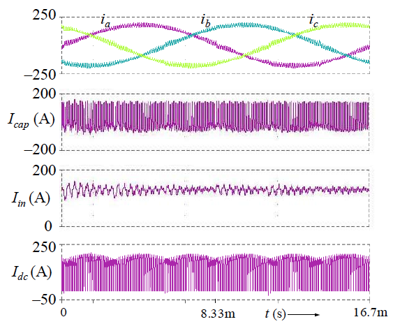
Fig. 2. Simulated input dc and output ac currents in three fundamental cycles.
The machine parameters of the induction motor used in this simulation are: pole = 2, stator resistance = 0.012 Ω, rotor resistance = 0.0125 Ω, magnetizing inductance = 3 mH, stator and rotor leakage inductance = 50 μH [4].
Notice that the inverter is controlled with the space vector modulation (SVM) scheme, with which one phase keeps un-switched over one-sixth of the line cycle, while the other two phases are switching at a pre-calculated duty-cycle pattern to ensure a sinusoidal current output.
Fig. 3 shows detailed current waveforms for five switching cycles. The gating signals of the switching devices are also shown to explain how the output ac currents are reflected back to dc link. When all the upper switches (S1, S3, S5) are turned on, as shown in a narrow shaded area, the motor terminal voltages are zero, and the currents circulate through diodes. Thus in this narrow shaded area, the dc link current is zero. In the wide shaded area, switch S5 remains on, but switch S3 turns off, and switch S6 turns on. This allows the load current to flow back to the dc link, i.e., the dc link current equals the load current, which is the maximum current among three phases. Thus, the dc link current Idc always fluctuates between zero and maximum load current in every switching period. With battery drawing a near constant dc input current Iin, the dc bus capacitor current Icap, sees a high frequency ac ripple current which is the difference between Iin and Idc. Under the simulated 37.5-kW output, which is the continuous rating of the tested motor, the capacitor rms current is 80 A, and the battery input current is 130 A. The ratio of the dc bus capacitor current Icap and the dc input current Iin is found to be 61.5%. It can be easily projected to show that at 75-kW maximum drive output condition, the capacitor rms current will be 160 A.
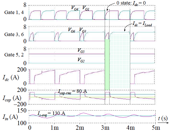
Fig. 3. Gating signals and inverter input dc currents.
Traditionally the size of Cdc has been chosen in an arbitrary basis. For commercial 75-kW traction motor drives, the value was found from 15 mF to 25 mF with electrolytic capacitors. The design philosophy with high-capacitance electrolytic capacitors is typically inherited from the design of industrial drives, where Cdc is calculated to smooth the 6th harmonic ripple caused by the utility line. According to the above simulation study, the need for smoothing 6th harmonic is no longer necessary when the source is a stiff battery stack, and the capacitor selection criterion should now be focused on the current handling capability but not the voltage ripple.
In addition to Cdc, there are some other capacitors that are traditionally used in an inverter to deal with parasitic components and switching problems. Fig. 4 shows detailed parasitic components of a traction motor drive. The passive components contained in dotted boxes in Fig. 4 are the parasitic components that are omitted in the circuit diagram, but are causing some unwanted effects in switching.
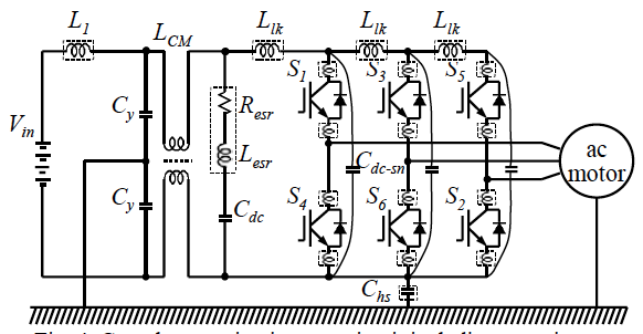
Fig. 4. Complete traction inverter circuit including capacitors needed and all the parasitic leakage inductances.
Take the parasitic inductance as example. The parasitic inductance exists between phase legs, Llk, and all the device connections. These inductances will induce a voltage spike during device switching. The magnitude of the voltage spike depends on the magnitude of the lumped parasitic inductance and the rate of current change. Physical size constraint makes it nearly impossible to eliminate parasitic inductance in a high power inverter. Thus, a dc snubber capacitor, Cdc-sn, is normally added across the top and bottom dc rails on each phase leg to suppress the voltage spike locally. The requirements for Cdc-sn are high peak current capability and extremely low inductance. Depending on layout and packaging, the lumped parasitic inductance ranges from 10’s to 100’s of nH. The leakage inductance and its interconnect inductance of Cdc-sn should be at least one order of magnitude less than the lumped parasitic inductance; otherwise, it will defeat the purpose of voltage spike suppression.
When electrolytic capacitors are used as Cdc, the above- mentioned Cdc-sn is unavoidable because the parasitic inductance in electrolytic is quite significant. However, with the use of the proposed low-inductance film capacitor and an integrated thick copper printer circuit board (PCB) layout, it is also possible to eliminate the dc snubber capacitor.
III. CAPACITOR CHARACTERISTICS
Although the selection criteria are first based on the current ripple capability and low inductance. There are other important features that need to be included in traction motor drive applications. The key features include:
- Operating temperature range from –55 °C to +105 °C.
- Dielectric strength (Maximum): 650 Vdc tested at 25 °C for 60 seconds.
- E.S.R. (Maximum): 0.003 Ω tested at 10 kHz, 25 °C
- E.S.L. (Typical): 21 nH
- Peak current (Maximum): 9818 A
- RMScurrent:207Aat10kHz,25°Cand147Aat 10 kHz, 85 °C
Fig. 5 shows the photograph of the dc bus capacitor specifically designed to meet the above-described features. Key features of its mechanical design are:
- Heat sinking plate: The bottom aluminum plate allows the heat sink to carry the heat away and maintain the capacitor operating temperature below the maximum heat sink temperature.
- Low profile: The rectangular block has a form factor similar to most of high-power IGBT modules, thus allowing the layout of dc bus bar largely simplified because the capacitor and IGBT modules can be mounted on the same heat sink plate to avoid bending the power bus bar.
- Heavy-duty studs: The studs are of 5/8” diameter and are made of copper with nickel plating. It allows 200-A continuous current flow without introducing significant temperature rise.
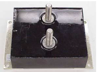
Fig. 5. Photograph of the high-current handling film capacitor.
Fig. 6 shows the capacitor maximum permissible current versus operating frequency at 55°C temperature condition. The curve indicates that the rms current rating increases with the frequency. In a dc source or battery powered inverter, the dc bus capacitor does not need to handle low frequency currents, but the high frequency ripple is the concern. The designed film capacitor shows more than 200-A rms current capability in the operating frequency and temperature ranges and is desirable for the specified 75-kW traction motor drive application.
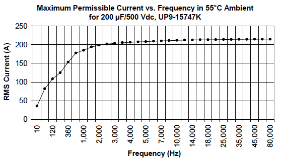
Fig. 6. Maximum permissible current.
Fig. 7 indicates that the rms current rating of the capacitor is deteriorated with the hot spot temperature. It should be noticed that with heat sinking plate the hot spots can be avoided, and the current handling capability can be maintained at a desirable level.
Fig. 8 indicates the capacitor impedance as a function of the frequency. The lowest impedance point is the resonant frequency that turns the capacitor characteristic into inductor. Any high frequency noise or ripple currents, especially the electromagnetic interference (EMI) related currents, will not be filtered by this dc bus capacitor. Thus, it is necessary to have additional smaller differential mode capacitors and common mode capacitors to filter the noise currents that have frequency beyond 80 kHz.
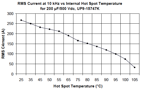
Fig, 7. Current rating as a function of the hot spot.
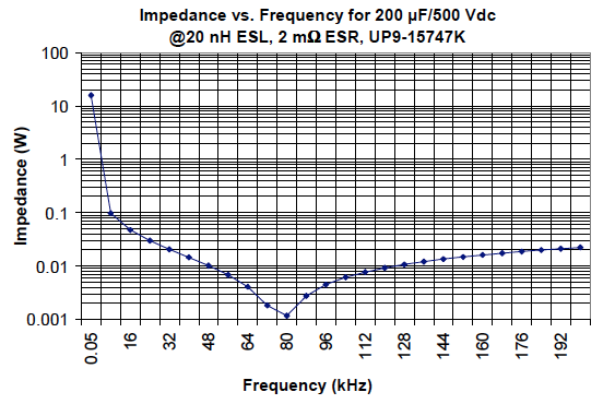
Fig. 8. Impedance as a function of frequency.
Fig. 9 shows the life expectancy of the dc bus capacitor. The traction motor drive inverters are typically running at an ambient or heat sink temperature of 65°C. With the temperature rise between 10 and 15 °C, the life expectancy is reduced to approximately half, or 100,000 hours. Such a life Cy span is still far superior to the electrolytic capacitors that are typically good for only 10,000 hours. In fact the life span of the designed film capacitor is much longer than the operating life of the vehicle operating life [2].
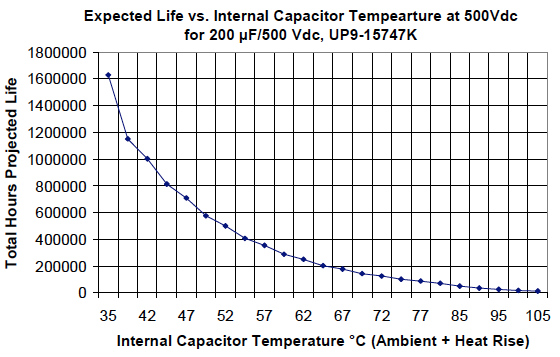
Fig. 9. Life expectancy as a function of temperature.
IV. A LOW-INDUCTANCE CAPACITOR BASED INVERTER AND EXPERIMENTAL RESULTS
Fig. 10 shows the photograph of an all film capacitor- based 75-kW inverter, which realizes the circuit shown in Fig. 2. A heavy-copper based multi-layer PCB replaces the conventional power bus bar. All the capacitors needed are mounted on the PCB either by studs or by soldering. Noticed that Cdc-sn and CCM are off-the-shelf products, and their voltage ratings are not optimized. The key to this package is the dc bus capacitor, Cdc, which is custom-built to handle high current at a high operating temperature environment. It has a base plate that allows heat sink mounting for convenient thermal management.
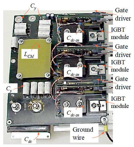
Fig. 10. Photograph of the inverter assembly.
Fig. 11 shows the experimental inverter output current and dc bus capacitor current waveforms at 13.7 kW output load condition. The output load current presents 10-kHz switching ripple on top of a sinusoidal wave. At 217-V dc bus voltage, the measured dc input current and the capacitor current are 69 A and 42.3 A, respectively. The ratio of Icap and Iin is found to be 61.3%, consistent with what was found in the simulation result.
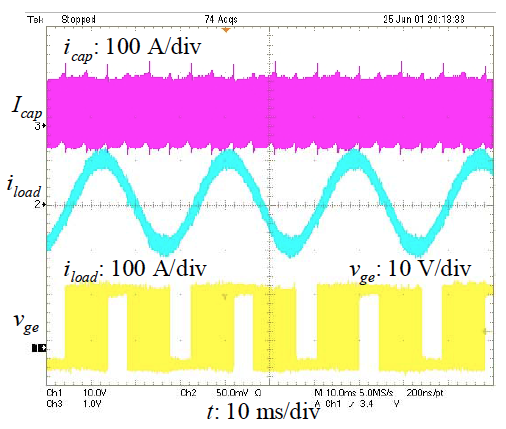
Fig 11. Experimental inverter output and dc bus capacitor currents.
Fig. 12 shows the experimental dc bus capacitor current with expanded time scales. The top trace of the upper window indicates the capacitor current over 2/3 fundamental cycle, and the top trace of the lower window indicates the capacitor current over two switching cycles. The capacitor gets charged when all the upper switches of the inverter are turned on; it is discharged when one upper switch is turned on, and at least one lower switch is turned on. The capacitor current wave shapes agree with the simulated result very well.
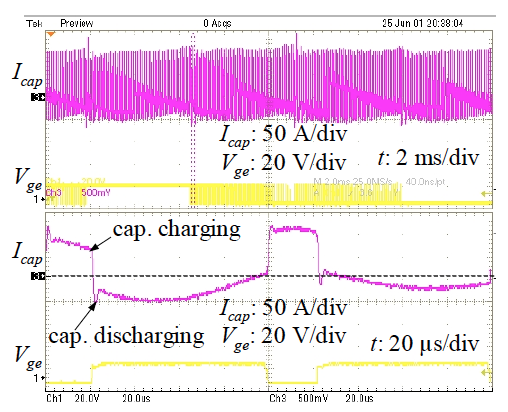
Fig. 12. Experimental dc bus capacitor current.
The capacitor current varies with different load current conditions. Fig. 13 indicates the measured dc bus capacitor current versus input dc current. As a rule of thumb, in this induction machine based traction motor drive, the dc bus capacitor ripple rms current is approximately 61% of the input dc current. This percentage agrees with the simulated results shown in Figs. 2 and 3. The result provides a good guideline for the dc bus capacitor design. Using the 75-kW, 300-V inverter as the design target, a dc bus capacitor with 150 Arms current handling capability at 65°C operating temperature is necessary.
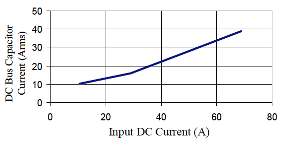
Fig. 13. Measured DC bus capacitor current versus input dc current.
The voltage spike due to device switching and parasitic inductance can be minimized by a good circuit layout and low-inductance dc bus capacitors. In a conventional copper bar based layout with high ESL electrolytic capacitor as the dc bus capacitor, the voltage spike is more than 30% of the dc bus voltage. With the use of multi-layer PCB as the power bus bar and the combination of high-frequency dc bus capacitor Cdc and dc snubber capacitor Cdc-sn, the voltage spike is largely reduced. Fig. 14 shows the experimental results with different configurations of Cdc and Cdc-sn.
Fig. 14(a) shows that the circuit operation without Cdc-sn but with the above-mentioned high-current low-inductance Cdc, the voltage overshoot is 56 V or 14% of the dc bus voltage, which is 400 V. Fig. 14(b) shows the results with Cdc + Cdc-sn. The Cdc-sn consists of two paralleled 1-μF high frequency film capacitors [5]. Each snubber capacitor used here has extended but fitted pads that can be mounted to the IGBT module. The voltage spike with this configuration drops to 38 V or 9.5%. Fig. 14(c) shows the test results with Cdc + Cdc-sn again, but the Cdc-sn does not have connecting pad. Instead, it has a set of fitting holes that allows the capacitor mounted directly on top of the IGBT module [6], as can be seen in Fig. 10. The capacitance value of this direct-mount Cdc-sn is 2 μF, and the resulting voltage overshoot is further reduced to 30 V or 7.5%. The comparison of these test results indicates the significance of layout and parasitic inductance reduction in voltage spike reduction.
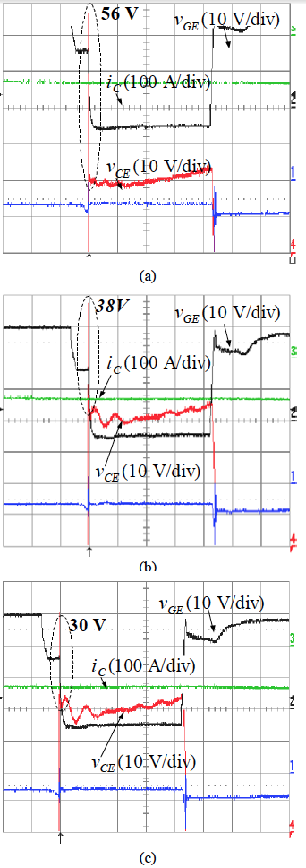
Fig. 14. Device voltage turn-off overshoot: (a) with Cdc but without Cdc-sn; (b) with Cdc and 2 × 1-μF Cdc-sn. (b) with Cdc and with a low-μ Cdc-sn.
Table 1 compares the voltage spikes in three different configurations. The first configuration applies to our first generation inverter design that has three 4,700-μF electrolytic capacitors and conventional copper bus bar layout. Its voltage spike is more than 33 % at the nominal voltage and current condition. Because this voltage spike is too high, it was not tested at 400 V condition. The second configuration is to use the recommended low-inductance high-current film capacitor. The result shows 15% at nominal voltage and current condition. The test condition was extended to 400-V bus voltage, and the voltage spike did not exceed the capacitor voltage rating. The last configuration is to add the 2-μF Cdc-sn on top of the IGBT, the voltage spike was cut down to less than 8%.
Table 1. Comparison of voltage spikes with different dc bus capacitors
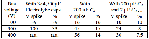
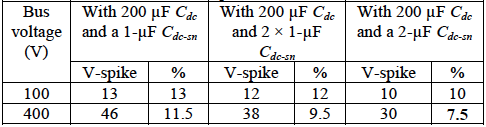
Table 2 compares the voltage spikes with the same 200- μF Cdc but three different Cdc-sn configurations. The first configuration has only one 1-μF pad-mounting capacitor. The resulting voltage spike is 11.5%. The second configuration has two paralleled 1-μF pad-mounting capacitors, and the resulting voltage spike is reduced to 9.5%. The last configuration is to add the through-hole mounting 2-μF Cdc-sn on top of the IGBT, and the voltage spike was cut down to 30 V or 7.5%.
Table 2. Comparison of voltage spikes with different sc snubber capacitors
Although the dc snubber capacitor helps reduce the device voltage overshoot, with the use of high-frequency film capacitor as the dc bus snubber and multi-layer PCB layout, the performance is already outstanding. By looking at Tables 1 and 2, the overshoot voltage reduction by replacing the electrolytic capacitor with the proposed high frequency film capacitor is significant enough that further voltage overshoot reduction from the dc snubber capacitor may not be needed. For performance consideration, further voltage spike reduction is preferred, but for cost consideration, it appears that Cdc-sn can be eliminated.
V. CONCLUSIONS
This paper has demonstrated the use of low-inductance high-current film capacitors in a high-power inverter for battery-powered traction motor drives. Both simulated and experimental current waveforms of the dc bus capacitor of a space vector modulated inverter indicate that the capacitor needs to handle high-frequency current with an rms value approximately 61% of the average dc bus current. Although this percentage differs among different machines and different modulation schemes, its magnitude is always nontrivial in most of inverter-motor drive systems. With such a high current flowing in the dc buc capacitor, it is apparently that the conventional design with the use of electrolytic capacitor not only is bulky in size, but also is inadequate in current handling.
Throughout extensive computer simulation and hardware implementation verification several conclusions can be drawn:
- The dc bus capacitor selection should be based on the current handling capability but not the voltage ripple in a battery-powered inverter drive system. The conventional design using multiple bulky electrolytic capacitors can thus be completely replaced with a single high-current film capacitor.
- The high-current film capacitor satisfies not only the ripple current requirement, but also the life expectancy needed in a traction motor drive.
- The high-current film capacitor exhibits low inductance, and thus the voltage overshooting during device switching can be substantially reduced.
- With low-inductance power bus bar design along with the use of low-inductance dc bus film capacitor, it is possible to eliminate the dc snubber capacitor for additional size and cost reduction.
ACKNOWLEDGEMENT
The authors would like to thank Dr. Charles E. (Bud) Konrad of VPT Inc. and Mr. James A. Merritt of the U. S. Department of Energy (DOE) for their strong support under the DOE Cooperative Automotive Research for Advanced Technology (CARAT) Program.
REFERENCES
[1] I. W. Clelland, “Recent Advances in Capacitor Technology with Application to High Frequency Power Electronics and Voltage Conversion,,” in Conf. Rec. of IEEE Applied Power Electronics Conference, Dallas, TX, March 1999, pp. 685 – 691.
[2] Jih-Sheng Lai, “Practical Design Methodology of Auxiliary Resonant Snubber Inverter,” in Conf. Rec. of IEEE Power Electronics Specialists Conference, Baveno, Italy, June 1996, pp. 432–437.
[3] Nichicon, Electronic Component Catalog, CAT8100L, 1998.
[4] T. Nergaard, J. S. Lai, H. Kouns, C. E. Konrad, “Optimal System Efficiency Operation of an Induction Motor Drive,” to be presented in IEEE IAS Annual Meeting, Oct. 2002.
[5] https://www.ecicaps.com/ECI_LOHENRY.htm, Electronic Concepts MP88 – Metallized Polypropylene IGBT Mountable Capacitor Datasheet.
[6] https://www.ecicaps.com/ECI_MP80.htm, Electronic Concepts MP80 Metalized Polypropylene IGBT Mountable Capacitor Datasheet.